A Thermal Solution for More Heat Dissipation per Dollar
Start Strategic PartnershipValue Statement
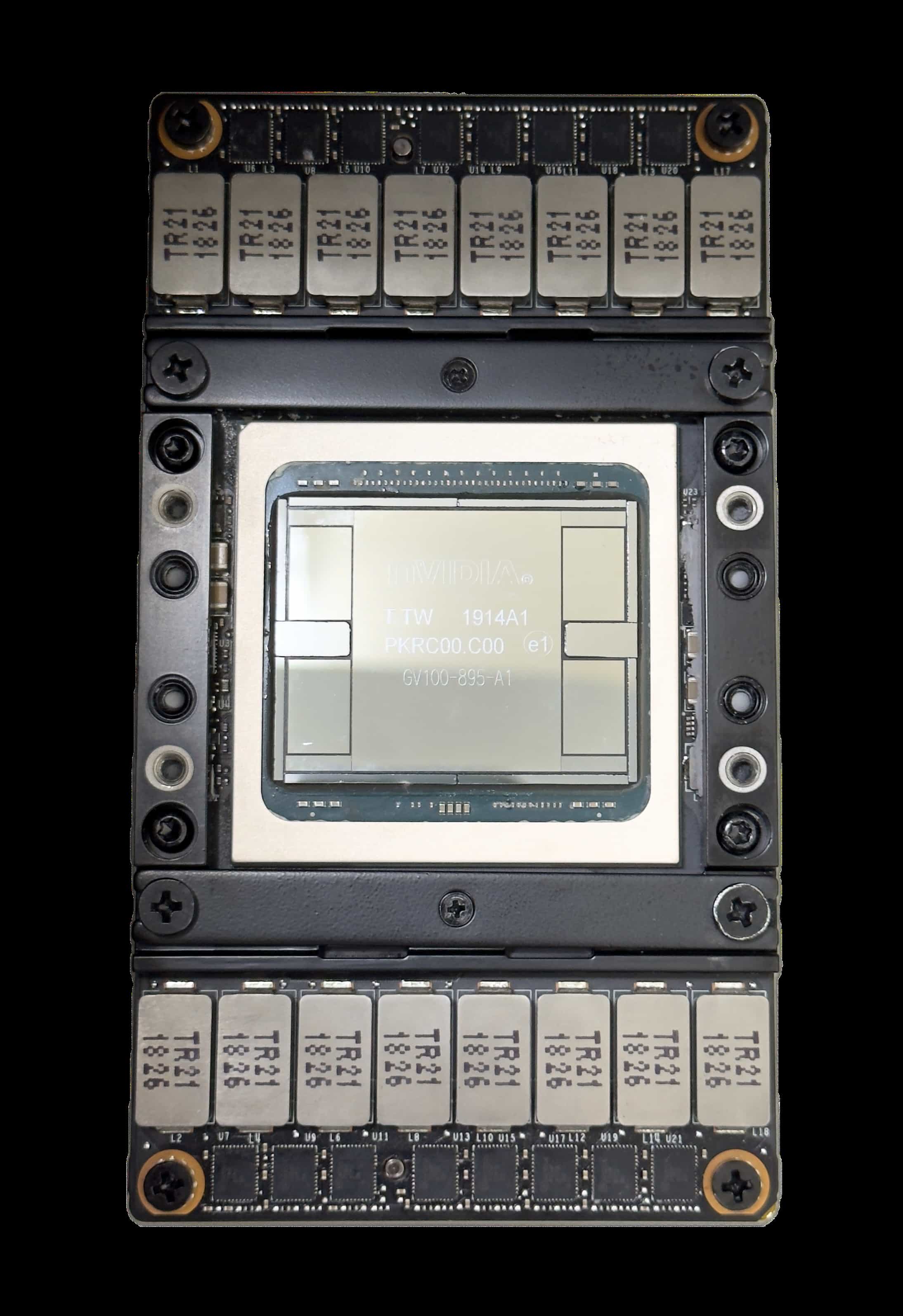
Manage package-level thermal loads with diamond–silicon composite components designed to fit existing architectures. Our customizable components draw heat away from the source more quickly, helping customers adopt new thermal-management technology with minimal design changes while keeping thermal costs under control.
Benefits
- Competitive price: A 12-inch diamond–silicon composite wafer costs less than twice the current market price of a 12-inch silicon wafer.
- High thermal conductivity: The composite delivers 600–900 W/m·K thermal conductivity.
- Fusion-bonding compatibility: With surface roughness (Ra) below 1.0 nm, the composite reduces contact thermal resistance by up to 99%.
- Low adoption barrier: The composite is designed for compatibility with existing architectures, allowing customers to adopt the technology with minimal design adjustments.

Overview
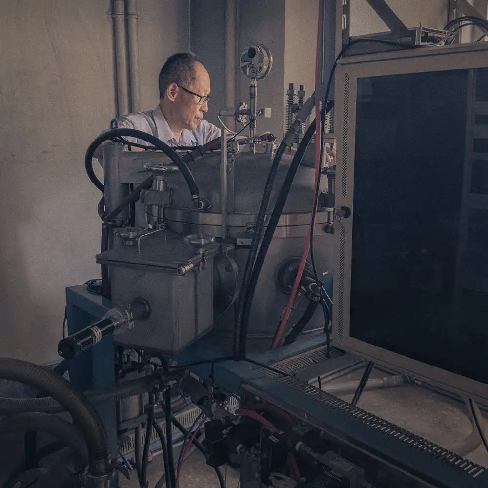
Our patent-pending diamond–silicon composite manages heat in advanced graphics processing unit (GPU) and high-bandwidth memory (HBM) applications. Before silicon infiltration, high-pressure, high-temperature diamond particles can be positioned across large areas, which gives manufacturers flexibility to customize designs.
Building on our experience commercializing single-layer diamond particle technology, we are expanding this approach for semiconductor packaging.
Start Strategic Partnership
email us at one.world@msa.hinet.net